Surface passivation of crystalline silicon solar cells has always been a top priority in design and optimization. The PERC/PERL design for passivated local open-pored contact with dielectric layers such as silicon oxide, aluminum oxide, and silicon nitride was introduced from the early back-field passivation only, to the front-side silicon nitride passivation, to the back side. Although this structure temporarily alleviated the problem of backside passivation, it was not eradicated and the high recombination rate at the opening remained, and the process was further complicated. In recent years, a technology that can achieve complete surface passivation on the backside and does not require open contact has become a hotspot for institutional research. This is Passivated Contact technology. It is also possible to implement a Selective Contact battery structure that does not require diffusion of the PN junction when both sides of the cell are passivated. This article will introduce in detail the background, characteristics and research status of the passivation contact technology, and discuss how to use this technology to achieve selective contact with the battery. Surface passivation evolution Passivated "prehistory" In the early days of commercial production of crystalline silicon cells prior to the 1990s, solar cell manufacturers have begun to adopt screen printing technology, but it is different from what we use today. The main difference lies in two points: First, the front screen printing silver paste had no fire-through function. Therefore, at the time of the production line, screen printing was required, and then the TiO2 antireflection layer was deposited. Another difference is that the silver paste at the time has poor ability to form effective ohmic contact with silicon, and only good contact with highly doped silicon is possible. Since TiO2 does not have a good passivation function, people did not consider excessive passivation at the time. Moreover, since the anti-reflection layer is on the metal electrode, the master gate needs to be covered with a stencil during deposition so that the subsequent string welding can be performed. Although this period, in the laboratory, researchers have used SiO2 to passivate the surface of the battery and achieved remarkable open circuit voltage and efficiency. SiNx:H first evolution In the 1990s, scientific institutions and manufacturers began to explore the use of plasma-enhanced chemical vapor deposition (PECVD) technology to prepare hydrogen-containing silicon nitride (SiNx:H) films as antireflection films on the front side of batteries. One of the reasons is the relatively suitable refractive index, but the more important reason lies in the excellent passivation effect of silicon nitride. In addition to saturation of surface dangling bonds, silicon nitride also reduces its interface state by its own positive charge, reducing the minority concentration in the positive n-type silicon, thereby reducing the surface recombination rate. The hydrogen carried in the SiNx can diffuse into the silicon during the sintering process to passivate the internal crystal defects of the emitter and the silicon wafer. This is particularly effective for lower quality polysilicon wafers, significantly increasing solar cell efficiency at the time. . Accompanied by innovations in passivation materials, changes in silver paste materials and sintering processes have also come at the same time. They are burn-through pastes and co-firing sintering processes. With the burn-through feature, the anti-reflection film can be deposited first, the screen printed on the screen, and then sintered. Due to the reversal of the sequence, there is no need to worry about the influence of the anti-reflection layer covering the metal grid lines on the welding, and the partial shielding required for deposition of TiO2 is also omitted. At the same time, people invented a co-firing process in which the slurry is sintered once and for all. In a single sintering process, the front silver paste is brought into contact with silicon through the SiNx, while the back aluminum paste also forms the back electrode and the back surface field simultaneously. ). This series of improvements greatly simplifies the process of screen printing batteries, and has gradually become the mainstream of crystal silicon battery production. Second evolution of AlOx As the passivation effect and contact performance of the front side of the battery are continuously improved due to the use of SiNx and improvement of silver paste, further optimization of the front has entered a bottleneck stage, and people have turned their sights to another compounded area, that is, the back surface of the battery. Although in conventional screen-printed crystalline silicon cells, the aluminum back-field can reduce the minority concentration and reduce the recombination, it still cannot be compared with the passivation effect brought by using the dielectric layer. In fact, the backside dielectric layer passivation is not a new topic. UNSW proposed the emitter and back passivation (PERC) structure and the emitter and back passivation local diffusion (PERL) structure as early as the 1990s. In early designs, this Both structures are passivated with a silicon oxide layer on the backside, with local openings to achieve point contact to reduce the area of ​​the non-passivated region. The difference between the two lies in whether local doping and diffusion are performed in the open area, local diffusion increases the difficulty of the process, but local back electric field is formed, and the recombination rate of the contact part is reduced. However, the growth of high-quality silicon oxide requires higher temperatures. For silicon wafers that have undergone high-temperature diffusion, in order to reduce the impact on the lifetime of the body and minority, the long-time high-temperature process should be minimized. Therefore, the search for other materials is in 2000. Years or so on the agenda. Since SiNx has proved many advantages on the front of the battery, can it continue to use this material on the back side? The answer is no, as mentioned above, one of the mechanisms of SiNx passivation is to use its positive charge to reduce the minority concentration of the positive n-type region, but on the back of the p-type, the positive charge will likely induce a layer on the backside. An inversion layer, which causes back-side shunt losses, affects current, and reduces voltage and fill factor. Then the question came, and which one was the passivation? Thanks to the efforts of several European research institutes, another material that is not new to photovoltaic researchers is once again on the stage. It is alumina (AlOx). It not only can passivate surface defects like SiNx, but also has a negative charge opposite to that of SiNx. Because of this, the use of an AlOx passivation layer on the back side of p-type silicon not only does not form an inversion layer and causes leakage, but increases. The multiple-substance concentration in p-type silicon reduces the minority concentration, thereby reducing the surface recombination rate. However, the use of AlOx also needs to be accompanied by improvements in this process and advances in equipment, such as solving the problem of high-speed deposition of AlOx, the inherent instability of alumina itself, and low yields. Passivation contact, the third evolution? PERC and PERL structure batteries already have a relatively complete surface passivation structure, but the back contact area is limited to the open area, in addition to increasing the complexity of the process, the process of opening the hole using a different process will also be on the surrounding Silicon materials cause varying degrees of damage, which additionally increases the recombination of the metal contact areas. Since the opening limits the carrier's transmission path, it deviates from the shortest path perpendicular to the contact surface and is congested at the opening, increasing the loss of the fill factor. Is there a way to reduce surface recombination without opening holes? This requires mention of Passivated Contact technology, which has been rising in popularity in recent years. Suppose we can find a material or structure that satisfies (1) having a good surface passivation effect; (2) separating quasi-Fermi energy levels; and (3) efficiently transporting a carrier. Then, this structure can be applied to the surface of the battery to form a passivation contact that satisfies passivation requirements and can transmit current without opening. The Fraunhofer Institute for Solar Energy has developed a project called TOPCon (Tunnel Oxide) Passivated Contact, tunneling oxide passivation contact) technology. The researchers first chemically prepared a thin layer of silicon oxide on the backside of the cell, and then deposited a thin layer of doped silicon that together formed a passivated contact structure. These two layers of material provided a good backside for the silicon wafer. The surface passivation, and because the oxide layer is very thin, the silicon layer is doped, many children can penetrate the two passivation layer, and the minority is blocked, if deposited on it, you can get without opening The passivation contact of the hole. The details of this technique will be discussed below. But can such passivation contact be used only on the back of the battery, what if it is used on the front? Solar cell without diffusion PN junction In fact, this is not a new problem, although the statement of passivation of the contact battery has only appeared in the past two years, but its description of the structure has indeed been fully studied by scientists. This kind of surface contact design that selectively passes through the carrier is realized by adding material and bending energy band of the structure instead of the battery absorbing layer itself. We call this Selective Contact battery. Our traditional understanding of the battery through the proliferation of PN junction is fundamentally different. Although we now have a common pn junction with a high-temperature diffusion cell, the built-in electric field of the pn junction is considered to be the power to separate the photogenerated carriers and allow the solar cell to generate electricity. In fact, solar cells do not necessarily have to have a clear PN junction. In the 1970s, Professor Martin Green proposed a metal-insulator-semiconductor (MIS) structure solar cell that does not need to diffuse PN junctions. In 1985, Professor Eli Yablonovitch proposed that the ideal solar cell should be "designed with two heterojunctions", that is, the absorbent material is placed between two wide bandgap materials. Dr. Richard Swanson, one of the founders of SunPower, also predicted that crystalline silicon solar cells with a theoretical efficiency approaching 10 years ago should “put a wide band gap material between silicon and metal to form a heterojunctionâ€. These structures all point to selective contact with the battery. Assuming that the absorber material is in the middle of FIG. 2 , the left and right sides are respectively a hole electrode and an electron electrode, and the electrode and the absorption material are a selective transmission layer. The left side is a hole transport layer and the right side is an electron transport layer. Because of the selective contact material's own bandgap, work function, and Fermi level, the absorber material is forced to bend, which allows only carriers that correspond to the selective transport layer to flow through and penetrate the interface while rejecting The other carrier, which in turn reduces the surface carrier concentration, results in a good surface passivation effect. Below, we explain the principle of the Panasonic Heterojunction (HIT) battery using the theory of selective contact [5]. The HIT cell absorber layer uses an n-type monocrystalline silicon wafer. First, a very thin intrinsic amorphous silicon layer is deposited on the front side as a surface passivation layer, and then a boron-doped p+-type amorphous silicon layer is deposited. Together, the two constitute a positive empty space. Hole transport layer. After deposition, the silicon wafer nears the surface due to the energy band bending, blocking the movement of electrons to the front surface, and the electrons can only move to the rear surface. In contrast to holes, although the intrinsic layer has a small barrier to holes, since the intrinsic layer is very thin, holes can tunnel and then pass through highly doped p+-type amorphous silicon. An intrinsic amorphous silicon layer and a phosphorus-doped n+ amorphous silicon layer are also deposited on the backside. Also due to energy band bending, holes cannot easily pass through the backside and electrons can pass through, so both constitute an electron transport layer. By depositing the selective transport layer on the positive and negative sides of the battery, the photo-generated carriers can only be enriched in the absorbing material and then flowed out from one surface of the battery, thereby achieving the separation of the two. Panasonic heterojunction HIT cells are a typical selective contact structure. Another typical selective contact cell is the Silevo Triex tunnel heterojunction cell [6], which is similar in structure to the HIT cell but uses silicon oxide instead of intrinsic amorphous silicon for the passivation layer. Unlike these two kinds of completely selective batteries, the above-mentioned backside passivated contact battery is actually a battery that selectively contacts only on the back side. What is the performance of the backside passivation contact technique, and is there a double-sided passivation contact technique used to achieve selective contact cell design? Let's take a look at the latest developments in this area. Research progress of passivation contact technology In recent years, several research institutions have successively conducted research on passivated contact solar cells. Although Panasonic has demonstrated the use of amorphous silicon thin films as passivation layers for HIT cells, the latest record-breaking efficiency is 25.6%. However, amorphous silicon thin films cannot withstand higher temperature follow-up processes because of their higher surface preparation requirements. Began to put the field of vision to other passive film materials. The current research hotspots of several research institutions have focused on the lamination of thin layers of silicon oxide and highly doped silicon. Fraunhofer ISE (Germany) Fraunhofer ISE has been cultivating for many years in the direction of passivated contact batteries. In 2013, it introduced its own tunnel oxide passivation contact (TOPCon) technology. Use an ultra-thin oxide layer with a doped thin film silicon passivated on the back of the cell. The back oxide layer has a thickness of 1.4 nm and is wet chemically grown. Subsequently, 20 nm of phosphorus-doped amorphous silicon was deposited over the oxide layer, followed by annealing to recrystallize and enhance the passivation effect. After the above steps, the open circuit voltage (iVoc) of a 200 μm-thick n-type FZ wafer with double-sided passivation can reach 710 mV or more, and even if the subsequent process temperature exceeds 400° C., the iVoc can be maintained at 700 mV or more. Silicon oxide reduces the surface state to maintain a lower tunneling resistance. Doped polysilicon provides field passivation and selective carrier transmission. It should be pointed out that in the study of early MIS batteries, researchers have discovered that when the thickness of the oxide layer exceeds 2 nm, the tunneling effect begins to decrease significantly, affecting the fill factor. Specific to the battery process, Fraunhofer ISE uses n-type FZ silicon wafers, the front using ordinary pyramid yarn, boron diffusion, ALD aluminum oxide and PECVD silicon nitride blunt stack to passivation and anti-reflection effect. The above-mentioned TOPCon technology is adopted on the back side, and the positive and negative metallization is realized by vapor-depositing Ti/Pd/Ag lamination. The open-circuit voltage of the battery reaches 690.4 mV, and the fill factor also reaches 81.9%. In order to further improve the efficiency, it further optimizes the design of the front electrode and reduces the metal contact area. The backside is replaced with a single layer of 1μm silver to improve the internal reflection on the backside, the open circuit voltage reaches 700mV, the fill factor is 82%, and the efficiency reaches 23.7%. At the SiliconPV conference in March this year, the latest efficiency of its use of TOPCon technology was 24.9%. Compared to PERL structure batteries, TOPCon technology eliminates the need for backside openings and alignment. In the above design, Fraunhofer ISE only uses TOPCon technology for the front. In 2014, the research institute announced the design of positive and negative passivation contacts to achieve the selective contact cell structure described above. Using a p-type FZ silicon wafer, 250 μm thick, without diffusion, a 1.4 nm oxide layer was directly chemically grown on both sides, and 15 nm phosphorus-doped and boron-doped amorphous silicon were deposited, followed by annealing. The front surface was sputtered with ITO, Ti/Pd/Ag was deposited on the stacking gate, and the back side was evaporated with silver as the backside electrode. The battery design has an open circuit voltage of 692.4mV and a fill factor of 79.4%. Due to the different annealing temperatures, the amorphous silicon deposited here does not crystallize as polysilicon, but instead reaches the microcrystalline silicon form in a similar thin-film silicon cell. However, due to the fact that the front is not napped, and the absorption of the front ITO and microcrystalline silicon layers in HIT-like batteries, the short-circuit current is only 31.6mA/cm2, and the efficiency is 17.3%. However, researchers have particularly compared the absorption of front-side polysilicon and microcrystalline silicon, and the absorption of microcrystalline silicon with the same thickness is up to twice as small as that of amorphous silicon. Therefore, the researchers believe that through the subsequent optimization, this structure is expected to become another selective contact battery design that can compete with HIT. National Renewable Energy Laboratory (NREL) NREL also uses silicon oxide and polysilicon films, which first diffuse the p-type emitter on the front side of the n-type silicon wafer, then use KOH to flatten the back surface, and then use a 700C thermal growth or nitric acid chemistry to make a silicon oxide layer about 1.5 nm thick. . A few tens of nanometers thick highly doped amorphous silicon (a-Si:H) is then deposited by PECVD. Through an annealing process of about 850C, the amorphous silicon thin layer is crystallized into polysilicon, and then subjected to 450° C. nitrogen-hydrogen mixed atmosphere annealing (FGA) to enhance surface passivation. The entire back side is metallized. NREL claims that SiO2 and polysilicon layers have an effect on the nature of passivation contacts. After the amorphous silicon recrystallization process at 850°C, the oxide layer obtained by chemical and thermal growth can get similar passivation effect, the open circuit voltage (ImpliedVoc) can reach 700mV or more, and the dark saturation current (Current) is less than 10fA/. Cm2, contact resistance is about 20-cm2. However, NREL believes that the mechanism of good quality of highly doped polysilicon/silicon oxide/silicon contacts is not fully understood. Good surface passivation may result from the chemical passivation effect of silicon oxide and the field passivation effect of highly doped polysilicon. The conductivity is then from the defect-assisted tunneling mechanism and micropores on the oxide layer. In addition, research institutes such as the Australian National University (ANU), the University of California (UC), and the Swiss Federal Institute of Technology in Lausanne (EPFL) are also conducting research in this area to explore different passivation materials and structures. In summary, the advantages of the backside passivated contact solar cell include (1) excellent backside passivation effect, completely eradicating the direct contact between the backside metal and silicon, and increasing the open circuit voltage, which is considered to be the current major compound loss of the solar cell. This is unavoidable with traditional aluminum back-field and PERC structures; (2) No complicated passivation layer opening process is required. If the passivation contact technology is applied to the front surface, the diffusion doping process can also be omitted to prevent the diffusion from affecting the carrier lifetime of the high quality silicon wafer, but it will also face the problem of positive parasitic absorption similar to that of the HIT cell, so the search for light absorption is less. The passivation film material is also one of the current research hotspots. Outlook It is also recalled that when selective emitters were just emerging, this technology solved the contradiction between silver pastes that require low-ohmic resistance regions to form ohmic contacts and square resistances that are too low and compound high. Although additional processes are required for diffusion in different regions, and subsequent processes require additional alignment, they are still given high hopes and are being tried. With the improvement of the paste, the front-side silver paste can form good contact with the higher and higher resistance silicon, and the uniform emitter diffusion concentration is reduced as a whole, which not only solves the selective emitter problem, but also avoids complicated problems. Processes have therefore been rapidly promoted and adopted. Selective emitter technology is not as popular as it used to be. Whether the backside will experience a similar path, although the PERC and PERL structure partially solve the problem of backside passivation, how to form local contact still brings about no small adjustment to the traditional screen printing production line. In contrast, passivation contact technology, although it does not need to open the hole to make the structure of the back of the battery more expensive, but the traditional crystalline silicon cell manufacturers lack the industrial experience of the thin film deposition and crystallization required for passivation contact technology, simple structure does not necessarily mean Simple production. Can the backside passivation contact technology come from behind, and the selective contact battery family is even more desirable due to the addition of double-sided passivation contact batteries. Will this technology have the ability to compete with HIT? Let's wait and see. In particular, it should be pointed out that under the combined influence of market demand and cost structure changes, even thin film companies like First Solar have acquired Tetrasun's crystalline silicon cells and components in recent years. Are domestic thin film photovoltaic manufacturers similar in their plans? With the accumulation of talents, technologies and equipment in amorphous silicon thin film deposition and crystallization, passivation contact technology or other selective contact technologies may be a good technology entry point for domestic thin film photovoltaic manufacturers to cut into crystalline silicon. Sodium Carboxymethyl Cellulose is a carboxymethylated derivative of cellulose, also known as cellulose gum, which is the main ionic cellulose gum. First made in 1918 and patented in 1921, it has since been commercialized in Europe. It was only for crude products and used as a gel and binder. In 1936 and 1941, the study of industrial applications was quite active and published several instructive patents. During world war ii, Germany will be used to synthesize detergent. Industrial production began in Germany in the 1930s with IG Farbenindustrie AG. Since then, the production process, production efficiency and product quality gradually improved. In 1947, the FDA confirmed that it was not toxic to the body, allowing it to be used as an additive in the food processing industry. Because of its many special properties, such as thickening, bonding, film forming, water holding, emulsification, suspension, etc., are widely used. In recent years, different qualities have been used in different fields of industry and people's lives. Sodium Carboxymethyl Cellulose Carboxymethylcellulose Sodium,Carboxymethyl Cellulose Sodium,Carboxymethyl Cellulose Sodium Cmc,Carboxymethyl Cellulose Sodium Nacmc Hebei pancan trading co. LTD , https://www.hbpancanshangmao.com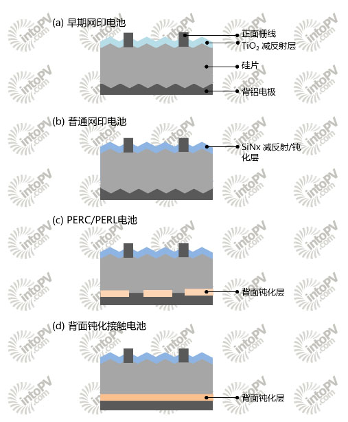
Figure 1. Evolution of surface passivation structure of solar cells 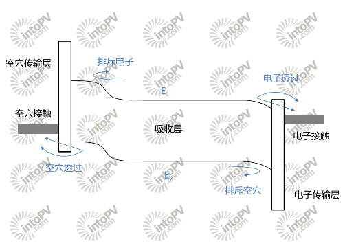
Figure 2, Selective Contact Battery Band Diagram 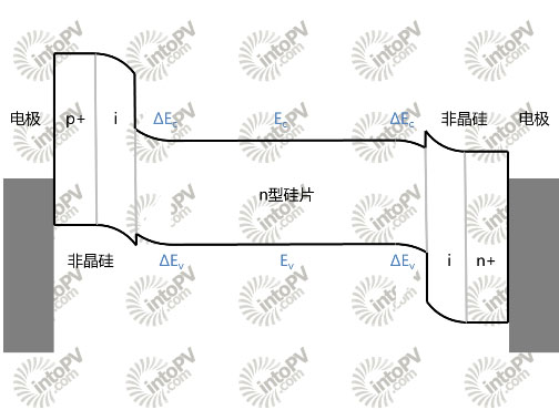
Figure 3, HIT Heterojunction Battery Band Diagram 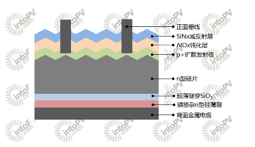
Figure 4. Backside passivated contact cell structure with TOPCon technology on the back 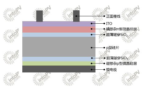
Figure 5. Selective contact cell structure with double passivation contact technology
