All semiconductor materials require purification of the raw materials, and the required purity is 6 "9" or more, up to 11 "9" or more. The purification method is divided into two categories, one is to purify without changing the chemical composition of the material, which is called physical purification; the other is to first purify the element into a compound, and then reduce the purified compound into an element, called Chemical purification. It is understood that physical purification methods include vacuum evaporation, regional refining, crystal pulling and purification, etc. The most used is regional refining. The main methods of chemical purification include electrolysis, complexation, extraction, rectification, etc. The most used is rectification. Since each method has certain limitations, a combination of several purification methods is often used to obtain a qualified material. Most semiconductor devices are fabricated on a single wafer or an epitaxial wafer with a single wafer as the substrate. Batches of semiconductor single crystals are all made by melt growth. The Czochralski method is the most widely used, and 80% of silicon single crystals, most of the germanium single crystals, and indium telluride single crystals are produced by this method, in which the maximum diameter of the silicon single crystal has reached 300 mm. The Czochralski method in which a magnetic field is introduced into the melt is called a magnetron crystal pulling method, and a highly uniform silicon single crystal has been produced by this method. A liquid covering agent is added to the surface of the crucible melt to be a liquid-sealed straight-drawing method, and a single crystal having a large decomposition pressure such as gallium arsenide, gallium phosphide or indium phosphide is drawn by this method. The melt of the suspension zone is not in contact with the vessel, and a high purity silicon single crystal is grown by this method. The horizontal zone melting process is used to produce tantalum single crystals. The horizontal orientation crystallization method is mainly used for preparing gallium arsenide single crystal, and the vertical orientation crystallization method is used for preparing cadmium telluride and gallium arsenide. The bulk single crystal produced by various methods is subjected to crystal orientation, barreling, reference surface, slicing, grinding, chamfering, polishing, etching, cleaning, detecting, encapsulating, etc., to provide a corresponding wafer. The growth of a single crystal thin film on a single crystal substrate is called epitaxy. Epitaxy methods include gas phase, liquid phase, solid phase, molecular beam epitaxy, and the like. Industrial production uses mainly chemical vapor phase epitaxy, followed by liquid phase epitaxy. Vapor phase epitaxy and molecular beam epitaxy of metal organic compounds are used to prepare microstructures such as quantum wells and superlattices. Amorphous, microcrystalline, and polycrystalline films are often formed on substrates such as glass, ceramics, and metals by various types of chemical vapor deposition, magnetron sputtering, and the like. Concerned about surprises Label: The range of semiconductor materials and the field of application Previous: Single beam suspension crane: purchase and safety of aerial work Next: What are the reasons for the high water temperature of diesel generator sets?
LED grow light with the COB packing technique being used,COB light source can save about 30% cost in the application, mainly lie in LED package cost,light engine production costs and the secondary light distributioncosts, which is great significance for applications and promotion of semiconductor lighting. Wecould also DIY the led ratio(wavelength ratio) which imitate the natural sun spectrum to help your plants grow in a very natural type of atmosphere, Absolutely, we are the very original and professional OEM/ODM factory, our lights have the great cost performance with the new integration technology being used for mass production, partners around the world keep telling us how amazed at the increase in output and the decrease in the energy bill.
Product Description
Item Display
Key Features
Plug with listed certificate safe to use.
The Plug you can choose
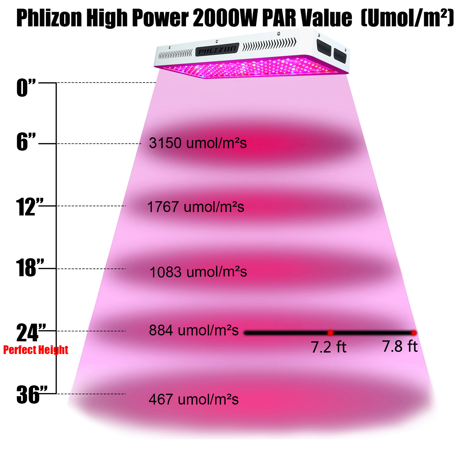
Full Spectrum COB LED Grow Light PAR Value
Applications
Our professional full spectrum COB LED grow light are suitable for all the indoor plants and good for seeding, growth,flowering and fruiting stages of plants, increasing the harvest and Saving energy.
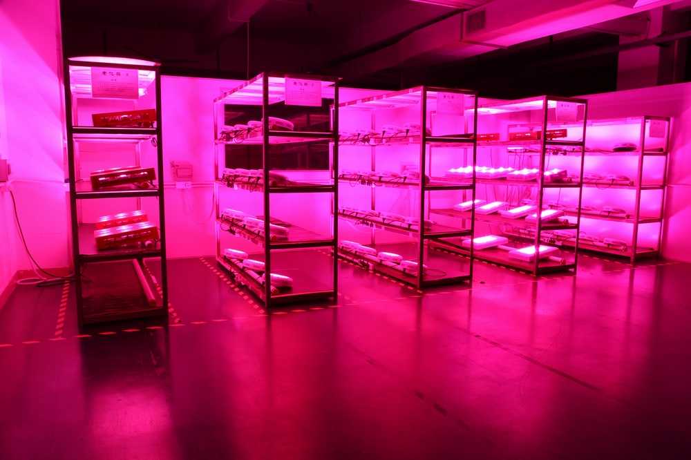
Our Ageing Test
Package
Cautions:
1.Do not use the lights in dripping water or anywhere where they will get wet, water and electricity can be a dangerous mixture
2. The working environment for the light is -20~40 degree celsius,45%RH~90%RH.
3. To protect the light, Plz cut off the power when there is a lightning strike.
4. Don`t touch or move when the light working.
Suggestions:
1.Clean the dust inside every 6 months to ensure the good heat dissipation and long life time.
2.Don`t keep too short distance to the plant canopy to avert leaves bleaching.
3. Highly hang the lamp will weaken the energy and affect the growth cycle of the plants, so the lamp should not be hang too high.
4. While taking care of the plants, please spray the leaves and branches 2-3 times everyday, to ensure the plants do not wrinkle a wither, and have no phenomenon of few fruit, and hard pericarp
Warranty
Philizon have over 6 years' experience in designing and manufacturing led grow lights. Persuiting to offer the best COB LED grow lights for plants growth, we cooperate with the scientific research institutes and the Academies of Agricultural Sciences in USA, Australia Canada, UK and so on.A great number of commercial plant growers test the lights, and their feedbacks show that this lamp owns a lot of 640nm,660nm and 740nm lights, which gives the plants enough nutrient in the flowering and fruiting phase and bring a far higher yield than other LED Grow Lights in the market.
COB LED Grow Light,COB LED Grow Lights,COB Grow Light,LED COB Grow Light Shenzhen Phlizon Technology Co.,Ltd. , https://www.szledplantgrowlights.com
Lower Price for Better Light, Definitely Worth Having.
Applies our patent COB(chip on board) tech,which brings more centralized lights source to plants growing and with a better heat dissipation system of led Grow Light.Innovated grow light wavelength,full spectrum,which has the same efficiency as CREE CXB3070 make your plants get better light and grow better


1.3years Manufacturer's Warranty for defective items within 3 years
2.We will guide you to fix it if gets small problems within 3 years
3.We will send you new items if the products are totally broken since technical or quality matters within 3 years
4.Retun and Refund: we provide 30days no question item return,we will refund all your money after we get the item,and we both provide 50% of the return shipping fee.
The scope and application of semiconductor materials
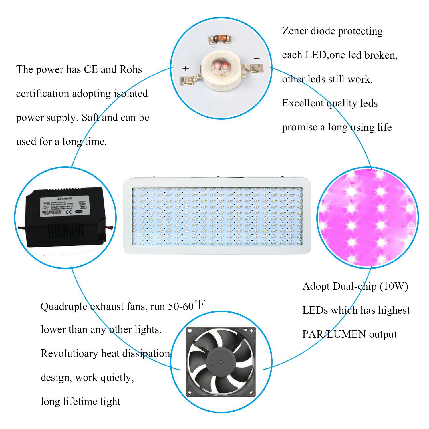
Upgraded Epistar chips,High Lumen,High penetration.
Zener Diode protection Each LED,one LED Out,other LEDs still work.
High quality material,Listed Certification Wires,Heatproof Tube,Zero-Risk to catch fire.
Efficient Full spectrum Special rations of Blue,Red and White for both blooming &fruiting stages.
Adopting isolated power supply,safe&easy to maintain&long life time.
Aluminum heat-conducting plate+high quality brand fans,efficient heat dissipation.
IR LED involved,it is not as bright as other leds,But promote the yield.